Eventually in most hobbyists’ path, one will end up working with high speed signals. These days so many microcontrollers support USB and even ones that don’t can use software USB. Of course using a microcontroller is the answer to every engineering problem, right? Most of us just work with USB 2.0 connected directly to a microcontroller for uploading and serial communications. With advent of the USB Tester, I have learned more about USB than I ever thought I would. Recently I have dived into USB 3. Which compared to 2.0, is so much more sensitive to your PCB routing as I found through trial and error. I have seen many projects on the various blogs and for sale on the usual sites that don’t follow or even try to route correctly. With USB 2.0 for the most part you can get away with it and it will still work. To help save you some time, I would like to share my findings that should help prevent PCB re-spins just due to USB not working. This is by no means an exhaustive guide to high speed routing as there are plenty of application notes across the web for that. I will list a few at the end of this post that I found helpful.
I am not by any means an expert on high speed signals, but I have learned enough to get the job done. In the end I was fortunate that my desktop PC had the first USB 3 controller made by Renasas which is much more sensitive than my laptop so I knew if it worked it would work for anyone.
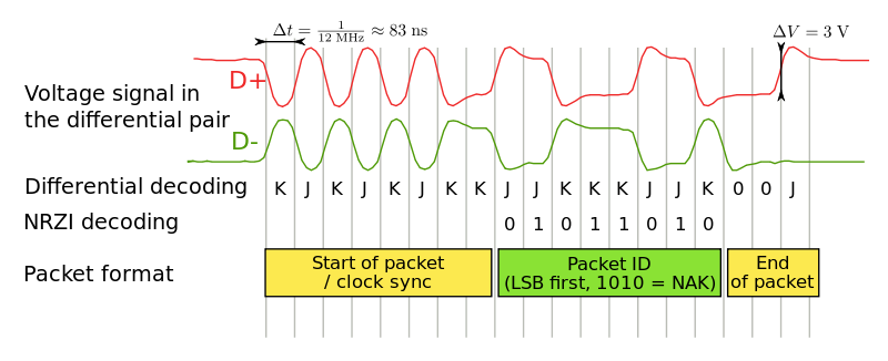
Diagram of USB Differential Pair (Wikipedia)
High speed signals use differential pairs instead of a single trace or a clock / data pair like I2C. By using a pair of traces you can cancel out noise. One is positive and the other negative. The idea is that electromagnetic interference would affect both signals and therefore would be canceled out since the receiving end looks at the difference of the two. Using a 2 channel oscilloscope you can connect to both signal and do a bit of math to see the resulting signal.
With USB 2.0 I was able to get away with branching (breaking out D+/D-). These are terms that you will come across with working with high speed signals.
Branching is when the traces are not direct from one point to another and have a split.
Stubs is if the signal hits a via with a pin in it from the top layer instead of the bottom layer to from a straight path.
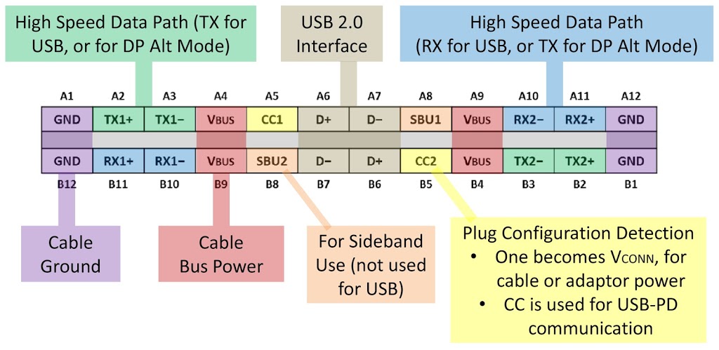
USB 2.0 only uses 1 differential pair vs USB 3 which uses 2 for full duplex operation. If you are using the Type-C connector you have duplicates of each pair plus for reversibility and extra signals for detecting orientation and other signal types.
USB Type-C Pin Out (Credit someone on the internet)
Important things to consider while laying out your board.
Calculate trace width and spacing to maintain 90Ohm differential (Calculator) This will also depend on the PCB you will be using. In my case OSHPark lists the specs of their PCB.
Maintain trace length of each pair. CAD tools have a differential pair routing tool along with meander to adjust traces for matching. A better way is to add a little length on the end of the short trace before connecting to your pad instead of having to meander which will affect the 90Ohm differential target. It can take a bit of time though to get it just right.
Use as few vias as possible as they affect signal integrity.
Route using 45degree angles instead of 90. I think this is to avoid reflections.
Avoid stubs by using a via before routing to a through hole part so you are on the bottom layer.
As much as possible, route above/below a continuous ground plane. On 2 layers boards this is pretty much impossible. With USB 3 it really should be a 4+ layer board.
Signals should be on the outer layers.
As always use the shortest path possible. (The Wozinack way ;))
Another one that may be hard to do is don’t cross signals above or below another signal. Ideally there should be a ground plane there anyway.
One way to avoid inverted pairs having to cross over each other is to mirror a part but then you have to deal with parts on both sides which may or may not be an issue for you. You should check with your assembly house if going that route. I have been able to reflow boards twice in this case. Surface tension usually keeps parts them from falling off.
Remember that higher speed signals travel along the skin of the copper so surface area is your friend and reduces impedance and attenuation on the signal. (More info)
Type-C cable only has 1 pair of differential pairs for USB 2.0 on the A side of the connector. B is unconnected. So I believe that means you should tie A and B together or maybe there is a mux IC for USB 2.0.
USB 3 Differential Pairs Example
It seems a lot to take in for a hobbyist but after awhile it starts to make sense. PCBs are getting cheaper so if it doesn’t work out you can keep trying different designs until it works.
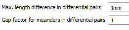
Here is my settings in Eagle CAD for a 2 layer board from OSHPark pictured above.
Eagle CAD Differential Trace Settings
Eagle CAD Length Settings
There is a minimum error in length but I always try to get it 100% matched.

Comments 1
awesome insight and guide, really helps, thank you!